
Chapter 13
13.3 Lead Controller Design – Solved Examples
13.3.1 Lead Controller Design – Solved Example 1
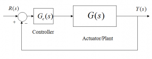
Consider a typical unit feedback closed loop control system, as shown, which is to operate under Lead Control.
The Lead Controller transfer function is as follows:
[latex]g_c(s) = K_c \cdot \frac{\tau s + 1}{\alpha\tau s +1} = \frac{a_1 s + a_0}{b_1 s + 1}[/latex]
Where [latex]\tau[/latex] is the so-called Lead Time Constant and [latex]a<1[/latex] The process transfer function G(s) is:
[latex]G(s)=\frac{0.5}{(s+5){(s+0.1)}^2}[/latex]
Open loop frequency response plots of G(s) are shown in Figure 13‑3. The closed loop performance requirements are: the Steady State Error for the unit step input for the compensated closed loop system is to be no more than 2%; Percent Overshoot of the compensated closed loop system is to be no more than 15%; the Settling Time, [latex]T_{settle(\pm 2 \%)}[/latex], is to be no more than 5 seconds – preferably less.
Check what the current (uncompensated system) values of the Phase Margin, [latex]\Phi_m[/latex], and the Crossover Frequency, [latex]\omega_{cp}[/latex], are. Estimate the uncompensated closed loop step response specs: Percent Overshoot, PO, Steady State Error, [latex]e_{ss(step\%)}[/latex], and Settling Time, [latex]T_{settle(\pm 2 \%)}[/latex]. Next, based on the specifications, calculate the required values of the Phase Margin for the compensated system, [latex]\Phi_{mc}[/latex], and the DC gain of the controller, [latex]K_{dc}[/latex].
Design the Lead Controller such that it meets the closed loop response requirements, and write the Lead Controller transfer function and its parameters. For your Controller, estimate the compensated closed loop step response specs: Percent Overshoot, PO, Steady State Error, [latex]e_{ss(step\%)}[/latex], Rise Time, [latex]T_{rise(100\%)}[/latex], and Settling Time, [latex]T_{settle(\pm 2\%)}[/latex].

SOLUTION:
Let’s start by finding the open loop DC gain – note that reading the gains off the Bode plots is difficult due to decibel units – here the gain could be read off from Figure 13‑3 as somewhere close to 20 dB. It is therefore, preferable to use the transfer function, if available, to compute the accurate gain values. Here we can compute the Uncompensated Open Loop DC gain – there is no controller, i.e. [latex]G_c(s)=1[/latex] – from the process transfer function:
[latex]K_{dcopen}=\lim_{s\rightarrow 0}G(s)=\lim_{s\rightarrow 0}\frac{0.5}{(s+5){(s+0.1)^2}}=\frac{0.5}{5\cdot0.01}=10[/latex]
The uncompensated closed loop DC gain is then:
[latex]K_{dc} = \frac{K_{dc0}}{1 + K_{dc0}} = \frac{10}{11}=0.9091[/latex]
The Phase Margin and the crossover frequency can be read off from the Bode plot in Figure 13‑3 as: [latex]\Phi_m = 33^{\circ}[/latex] and [latex]\omega_{cp} = 0.3[/latex] rad/sec. The damping ratio [latex]\zeta[/latex] and the frequency of natural oscillations [latex]\omega_n[/latex] for the uncompensated closed loop system can now be estimated by either reading it off the Phase Margin graph in Figure 12‑9, or by using the formula:
[latex]\zeta = \frac{\tan\Phi_m}{2\sqrt{\sqrt{({\tan\Phi_m)}^2 + 1}}} \rightarrow \zeta=0.3[/latex]
[latex]\omega_n=\frac{\tan\Phi_m\cdot\omega_{cp}}{2\zeta}=0.328[/latex]
[latex]G_m(s)=K_{dc}\frac{\omega_n^2}{s^2 + 2\zeta s + \omega_n^2}[/latex]
The uncompensated closed loop model based on the Open Loop Frequency Response is then:
[latex]G_{mu}(s) = \frac{0.0979}{s^2 + 0.1982s + 0.1077}[/latex]
Model specs can be calculated as:
[latex]PO = 100\cdot \left ( e^{\frac{-\zeta\pi}{\sqrt{1-\zeta^2}}} \right ) = 37\%[/latex]
[latex]T_{settle(\pm2\%)}=\frac{4}{\zeta\omega_n}=40.4[/latex]
[latex]T_{rise(100\%)}=\frac{\pi - \cos\zeta^{-1}}{\omega_n\sqrt{1-\zeta^2}}=6[/latex]
[latex]T_{rise(100\%)}=\frac{\pi - \cos\zeta^{-1}}{\omega_n\sqrt{1-\zeta^2}}=6[/latex]
[latex]G_{cl}(s) = \frac{0.5}{s^3+5.2s^2+1.01s+0.55}[/latex]
[latex]G_{cl}(s) = \frac{0.5}{(s+5.02)(s^2+0.1793s+0.1095)}[/latex]
The closed loop transfer function has a dominant pair of complex poles, with the damping ratio [latex]\zeta=0.27[/latex] and the natural frequency of oscillations [latex]\omega_n=0.33[/latex] rad/sec, which are close to the model estimates: [latex]\zeta=0.3[/latex], [latex]\omega_n=0.33[/latex] rad/sec. The actual transfer function also has a real pole at – 5.02, which is negligible, compared to the dominant pair of closed loop poles at [latex]-0.09\pm j0.32[/latex]. Thus, the assumed model is quite accurate – see the actual step response comparison, shown in Figure 13‑4, Figure 13‑30, and the calculated specs.

Actual specs, compared to the model specs (based on uncompensated Open Loop Bode plots), are:
| Actual Uncompensated System | [latex]G_{mu}(s)[/latex] – Model for the Uncompensated System | |
| PO | 41% | 37% |
| [latex]e_{ss(step\%)}[/latex] | 9.1% | 9.1% |
| [latex]T_{rise(0-100\%}[/latex] | 6.0 sec | 6.0 sec |
| [latex]T_{settle(\pm 2\%)}[/latex] | 42.0 sec | 40.4 sec |
The specs estimates from the model are very accurate, with all specs meeting the required values.
Now, the Lead Controller design – we can choose a simplified design or an analytical design. First, always calculate the required DC gain of the controller – this part is the same in both approaches.
Based on the required error specification:
[latex]e_{ss(step)c}=2\% \rightarrow \frac{1}{1+K_{posc}} = 0.02[/latex]
[latex]K_{posc}=\frac{1}{0.02}-1\rightarrow K_{posc}=49[/latex]
The compensated closed loop DC gain should be:
[latex]K_{dc(comp)} = \frac{K_{posc}}{1+K_{posc}} = \frac{49}{50}=0.98[/latex]
The controller DC gain is then:
[latex]K_c = a_0 = \frac{K_{posc}}{K_{posu}}=\frac{49}{10}=4.9[/latex]
Next, “translate” the required PO spec into the equivalent closed loop damping ratio. For PO = 15%, the required damping ratio, based on Figure 7‑4, is [latex]\zeta = 0.517[/latex]. The compensated Phase Margin should be, based on Figure 12‑9: [latex]\Phi_{m(comp)}=52^\circ[/latex]. Let’s round off the Phase Margin to: [latex]\Phi_{m(comp)}=55^\circ[/latex]. Next, “translate” the required Settling Time spec into the equivalent closed loop frequency of natural oscillations:
[latex]T_{settle(\pm2\%)} \frac{4}{\zeta\omega_n}=5 \rightarrow \omega_n=1.55[/latex]
That frequency can then be “translated” into the minimum required Phase Margin crossover frequency:
[latex]\omega_{cp} = \frac{2\zeta\omega_n}{\tan(\Phi_m)} = \frac{2\cdot0.517\cdot1.55}{\tan(55^\circ)}=1.12[/latex]
What do we do next? The two approaches differentiate on how we proceed.
13.3.1.1 Lead Controller Design Solved Example 1: The “Simplified” Lead Design
Based on the required PO spec, let’s decide on the “good” Phase Margin for the compensated system – it will be [latex]\Phi_{m(comp)}=55^{\circ}[/latex]. Next, based on the required Settling Time spec, let’s decide on a “good” crossover frequency – let us pick [latex]\omega_{cp}=1.5[/latex]. Remember that it is an arbitrary choice that does not guarantee that the solution is the “best”, or “optimal”. It will result in one possible improvement of the system response. Note that in the Lead Design, the compensated crossover frequency will always be to the right of the uncompensated frequency of the crossover. If it were to the left of the uncompensated frequency of the crossover, we would end up with a Lag Design.
At the chosen frequency of 1.5 rad/sec, we need to find the magnitude and phase of the original system G(s). Recall that reading values off the dB plot is notoriously inaccurate, and thus it is better to substitute [latex]s=j1.5[/latex] into the transfer function G(s) to obtain more accurate values of magnitude and phase:
[latex]\left |G(j1.5)\right | = 0.042 \frac{V}{V} = -27.5dB[/latex]
[latex]\angle G(j\omega) = -189^{\circ}[/latex]
Recall that we are gaining the most phase “lead” at the mid-point frequency of the Lead Controller (see the graph below). That mid-point will become our intended compensated crossover frequency, at which the Phase Margin will be measured. If we want to [latex]\Phi_{m(comp)}= 55^{\circ}[/latex], then the required “phase lift” at [latex]\omega_{cp}= 1.5[/latex] would be:
[latex]\theta=-180^{\circ}+\Phi_m - \angle G(j1.5) = -180^{\circ} + 55^{\circ} + 189^{\circ}=64^{\circ}[/latex]
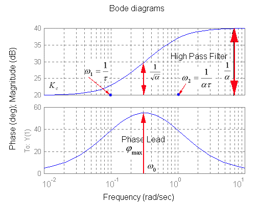
We will get that phase lift from the largest phase gain of the Lead Controller:
[latex]\varphi_{max} = \sin^{-1}\left (\frac{1-\alpha}{1+\alpha} \right ) = 64^{\circ} \rightarrow \alpha = 0.053[/latex]
The mid-point frequency of the Lead Controller is equal to 1.5 rad/sec:
[latex]\omega_0 = \frac{1}{\sqrt\alpha \cdot\tau} = 1.5 \rightarrow \tau = 2.896[/latex]
As seen on the plot, there is a gain increase at the mid-point frequency of the Lead Controller, equal to:
[latex]\frac{1}{\sqrt{\alpha}} = 4.34[/latex]
Further, remember that since we are going to use the DC gain of 4.9, the new total gain at the chosen crossover frequency of 1.5 is going to be the original gain of [latex]G(j1.5)[/latex] multiplied by 4.9 and by 4.34:
[latex]G_{new}(j1.5) = G_{old}(j1.5) \cdot 4.9 \cdot4.34=0.042\cdot4.9\cdot4.34=0.9[/latex]
To make that point the compensated crossover frequency, the total “new” gain has to be equal to 0 dB (1 V/V) – thus we can calculate the additional required adjustment of the DC gain of the controller equal to 1/0.9. The total DC gain of the controller is equal to 4.9/0.9 = 5.43. Note that, should the adjustment require a reduction of the controller DC gain, we would not be meeting the error specs, which would require reconsidering our choice of the crossover frequency.
The controller transfer function is:
[latex]G_c(s)=K_c\cdot\frac{\tau s + 1}{\alpha\tau s +1} = 5.43\cdot\frac{2.89s+1}{0.053\cdot2.89s + 1} = 5.43\cdot\frac{2.89s+1}{0.154s + 1}[/latex]
[latex]G_c(s)=\frac{a_1 s + a_0}{b_1 s + 1} = \frac{15.73s + 5.43}{0.265s +1}[/latex]
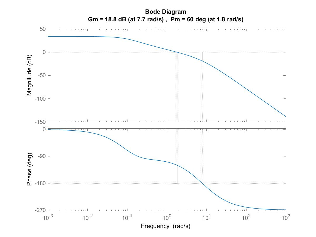
The open loop Bode plots before and after compensation and the system Phase Margin are shown in Figure 13‑22 and the compensated Phase Margin is shown in – it is [latex]\Phi_m = 55^{\circ}[/latex] at the frequency of [latex]\omega_{cp(comp)}=1.5[/latex] rad/sec, as was chosen for this design.

The expected compensated closed loop response specs can be estimated using the dominant poles model again. Use the formula or read off the Phase Margin graph:
[latex]\zeta = \frac{\tan\Phi_m}{2\sqrt{{(\tan\Phi_m)^2 +1}}} \rightarrow \zeta=0.54[/latex]
[latex]\omega_n = \frac{\tan\Phi_m\cdot\omega_{cp}}{2\zeta} = 1.98[/latex]
The compensated open loop gain:
[latex]K_{pos}=\lim_{s\rightarrow 0} G_{open}(s) = \lim_{s\rightarrow 0} G_{c}(s) \cdot G_(s) = 5.3\frac{0.5}{5\cdot0.01} =54.32[/latex]
The compensated closed loop gain:
[latex]K_{dc} = \frac{K_{dco}}{1 + K_{dco}} = \frac{54.32}{55.32} = 0.982[/latex]
The compensated closed loop model:
[latex]G_{mc}(s)=\frac{3.852}{s^2+2.142s +3.923}[/latex]

Model specs can be calculated as:
[latex]PO = 100 \cdot \left(e^{\frac{-\zeta\pi}{\sqrt{1-\zeta^2}}} \right ) = 13.27\%[/latex]
[latex]T_{settle(\pm2\%)}=\frac{4}{\zeta\omega_n}=3.73[/latex]
[latex]T_{rise(100\%)} = \frac{\pi-cos\zeta^{-1}}{\omega_n\sqrt{1-\zeta^2}}=1.286[/latex]
[latex]e_{ss(step\%)}=\frac{1}{1 + k_{pos}}\cdot100\%=\frac{1}{1 + 31}\cdot 100\% = 1.8\%[/latex]
The actual closed loop transfer function is:
[latex]G_{cl}(s) = \frac{51.246(s+0.345)}{(s+8.33)(s+0.3924)(s^2+2.993s+5.514)}[/latex]
As we can see, the actual closed loop transfer function has a dominant pair of complex poles at [latex]-1.5\pm j1.81[/latex], with the damping ratio [latex]\zeta=0.637[/latex] and the natural frequency of oscillations [latex]\omega_n = 2.35[/latex]rad/sec, as well as a zero at -0.3453 and two real poles at –8.33 and at -0.3924. The dominant poles model is not as accurate as before, because now an additional pole-zero combo shows up, closer to the Imaginary axis than the real coordinate of the dominant pair, and they do not totally cancel out. Their net residual effect on the closed loop response is that there is a slight additional overshoot caused by the zero, and the Settling Time is actually a bit slower than expected – see the actual step response comparison in Figure 13‑7 and the comparison of the specs below.
Actual specs, compared to the model specs (based on compensated Open Loop Bode plots), are:
| [latex]G_{mc}(s)[/latex] – Model for Compensated System | Actual Compensated System | |
| PO | 13.3% | 16.8% |
| [latex]e_{ss(step\%)}[/latex] | 1.8% | 1.8% |
| [latex]T_{rise(0-100\%)}[/latex] | 1.29 sec | 1.25 sec |
| [latex]T_{settle(\pm2\%)}[/latex] | 3.7 sec | 5.5 sec |
We could try to improve on this design by trying a different choice of the crossover frequency. The biggest problem is that a different choice of the crossover frequency may require us to make a final adjustment to the DC gain of the open loop (the one we need to make the total open loop gain equal to 0 dB at the crossover frequency) to be less than 1, and that will cause us to miss the steady state specs, requiring yet another iteration. However, it is much easier to meet all conditions using the analytical design formulae, which we will try next.
Plus of the simplified design – it will never lead to negative values of the controller parameters, which may happen with the Analytical Lead Design.
Minus of the Simplified Lead Design – some choices of the crossover frequency may result in the final adjustment of the open loop DC gain that will not meet the error specs. As well, Lead Design always results in adding a zero to the closed loop transfer function that is not totally cancelling out and thus is affecting the shape of the closed loop response by increasing its PO. The solution to both these problems is a trial & error approach to finding an acceptable set of controller parameters, but it is tedious.

13.3.1.2 Lead Controller Design Solved Example 1: The “Analytical” Lead Design
The analytical design gives us more flexibility to shape the open loop response by choosing different locations for the crossover frequency and quickly checking the resulting open loop parameters and the closed loop response.
Remember that the first step is always to choose the required DC gain based on the error specs – the calculations are identical to the simplified method, so the Controller DC gain ([latex]a_0[/latex]) will be the same.
Based on the required error specification:
[latex]e_{ss(step)c} = 2\% \rightarrow \frac{1}{1+K_{posc}}=0.02[/latex]
[latex]K_{posc}=\frac{1}{0.02}-1 \rightarrow K_{posc}=49[/latex]
The compensated closed loop DC gain should be:
[latex]K_{dc(comp)} = \frac{K_{posc}}{1+K_{posc}}=\frac{49}{50}=0.98[/latex]
The controller DC gain is then:
[latex]K_c = a_0 = \frac{K_{posc}}{K_{posu}} = \frac{49}{10} = 4.9[/latex]
Next, we pick the Phase Margin – in this example, we decided to have the Phase Margin of [latex]55^{\circ}[/latex], so let’s stick with this value. Next, we need to choose the crossover frequency – as long as it is more than 0.3 (the uncompensated value). First, let’s choose the same value as in the simplified design:
[latex]\omega_{cp(comp)} = 1.5 rad/sec[/latex]
To use the derived formulae for the controller constants [latex]a_1[/latex] and [latex]b_1[/latex], we need to find the uncompensated open loop Bode plot the phase and the gain at that frequency. Recall that reading values off the dB plot is notoriously inaccurate, and thus it is better to substitute [latex]s=j1.5[/latex] into the transfer function G(s) to obtain more accurate values of magnitude and phase – we already did that for the simplified design:
[latex]\left | G(j1.5) \right | = 0.042 \frac{V}{V}=-27.5dB[/latex]
[latex]\angle G(jw) = -189^{\circ}[/latex]
Next, substitute these values into the formulae:
[latex]\theta = -180^{\circ} + \Phi_m -\angle G(j1.5) = -180^{\circ}+55^{\circ}+189^{\circ} = 64^{\circ}[/latex]
Note that the “lift” angle is similar to the “maximum phase lift” in the simplified design, except that we don’t need to choose just this one maximum value, as you will see later. Next, we substitute the values into the Analytical Design formulae:
[latex]a_1 = \frac{1-a_0 \cdot \left |G(j\omega_{cp}) \right |\cdot\cos\theta}{\omega_{cp} \cdot \left |G(j\omega_{cp}) \right |\cdot\sin\theta}=15.9[/latex]
[latex]b_1 = \frac{\cos\theta-a_0 \cdot \left |G(j\omega_{cp}) \right |}{\omega_{cp} \cdot\sin\theta}=0.17[/latex]
These values are very close to the ones obtained using the simplified approach, as expected. The closed loop response will also be similar. Recall that that design had more Percent Overshoot than expected, and a longer Settling Time, so let us look for an improvement.
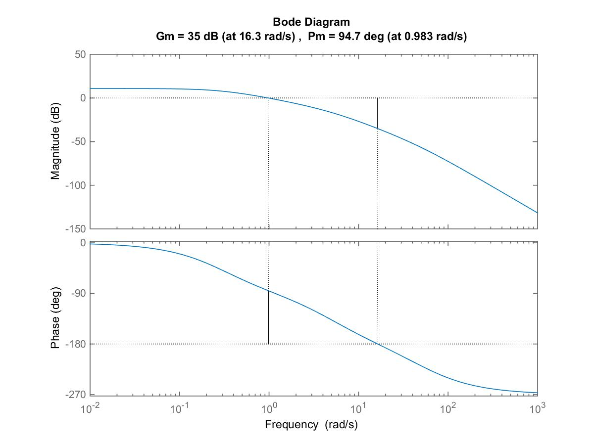
With the analytical design, we can easily choose a different frequency of the crossover (as long as it is more than the uncompensated crossover frequency of 0.3 rad/sec) and see if the resulting closed loop step response simulations will improve. Knowing that the Lead design causes more PO than expected, we can also overcompensate slightly for it by making the Phase Margin larger than the dominant poles model suggests. Let’s say, make [latex]\omega_{cp(comp)} = 1.8[/latex] rad/sec and [latex]\Phi_{m} = 60^{\circ}[/latex] . Again, we need to find the gain of the uncompensated system at that frequency (1.8 rad/sec) – recall that reading it off the graph is inaccurate so it is best to substitute [latex]s=j1.8[/latex] into G(s):
[latex]\angle G(j1.8) = -193^{\circ}[/latex]
[latex]\left | G(j0.2) \right | = 0.029 \frac{V}{V} = -30.8dB[/latex]
Next, substitute these values into the formulae:
[latex]\theta = -180^{\circ} + \Phi_m - \angle G(j0.2) = -180^{\circ} +60^{\circ}+193^{\circ} = 73^{\circ}[/latex]
[latex]a_1 = \frac{1-a_0 \cdot \left |G(j\omega_{cp}) \right |\cdot\cos\theta}{\omega_{cp} \cdot \left |G(j\omega_{cp}) \right |\cdot\sin\theta}=19.21[/latex]
[latex]b_1 = \frac{\cos\theta-a_0 \cdot \left |G(j\omega_{cp}) \right |}{\omega_{cp} \cdot\sin\theta}=0.083[/latex]
Here we see that the controller coefficients are acceptable, both being positive. Recall that the controller pole in RHP would be unacceptable, because it means an unstable open loop transfer function – even if the resulting closed loop is stable, for safety reasons we do not want to implement that – in case if the closed loop incidentally opens (a malfunction), we would have an unstable system on our hands. The RHP location of the controller zero would also be unacceptable – even if the controller pole is in a stable location, the RHP zero will introduce an effective delay into the system, extending both the Rise Time and the Settling Time. Recall that we will never get that kind of surprise in the “simplified” lag design. Let’s check the compensated system response. The open loop Bode plots before and after compensation are shown in Figure 13‑8 and the system Phase Margin is shown in Figure 13‑9. The controller transfer function is:
[latex]G_c(s) = \frac{a_1 s + a_0}{b_1 s + 1} = \frac{19.21s + 4.9}{0.083 s + 1}[/latex]
The expected compensated closed loop response can be estimated using the dominant poles model again. Use the formula or read off the Phase Margin graph in Figure 12‑9:
[latex]\zeta = \frac{\tan\Phi_m}{2\sqrt{\sqrt{(\tan\Phi_m)^2 + 1}}} \rightarrow \zeta = 0.612[/latex]
[latex]\omega_0 = \frac{\tan\Phi_m\cdot\omega_{cp}}{2\zeta} = 2.546[/latex]
The compensated closed loop model:
[latex]G_{mc}(s) = \frac{6.35}{s^2 + 3.18s + 6.48}[/latex]
Model specs can be calculated as:
[latex]PO = 100\cdot \left ( e^{\frac{-\zeta \pi}{\sqrt{1-\zeta^2}}} \right ) = 8.8\%[/latex]
[latex]T_{settle(\pm2\%)}=\frac{4}{\zeta\omega_n} = 2.57[/latex]
[latex]T_{rise(100\%)}=\frac{\pi - \cos\zeta^{-1}}{\omega_n\sqrt{1-\zeta^2}} = 1.11[/latex]
[latex]e_{ss(step\%)} = \frac{1}{1+K_{pos}}\cdot100\% = \frac{1}{1+49}\cdot100\% =2\%[/latex]

The actual closed loop transfer function:
[latex]G_{cl}(s) = \frac{115.75 (s + 0.2551)}{(s+13.13)(s+0.2688)(s^2 + 3.852s + 8.536)}[/latex]
Note that the closed loop model based on the dominant poles is now more accurate than in the case of the “simplified” design – while the additional pole-zero combo still shows up, both closer to the Imaginary axis than the complex pair of poles at [latex]-1.93\pm j2.2[/latex], their net effect on the closed loop response is almost negligible because of a much better “near-cancellation”: we have a zero at -0.2551, and a pole at -0.2688. Before they were at -0.3453 and at -0.3924, respectively.
See the actual step response comparison in Figure 13‑10 and the comparison of the specs below. The actual specs, compared to the model specs (based on compensated Open Loop Bode plots), are:
| Actual Compensated System | [latex]G_{mc} (s)[/latex] – Model for the Compensated System |
|
| PO | 10.5% | 8.8% |
| [latex]e_{ss(step\%)}[/latex] | 2% | 2% |
| [latex]T_{rise(0-100\%)}[/latex] | 1.1 sec | 1.1 sec |
| [latex]T_{settle(\pm 2\%)}[/latex] | 12.1 sec | 5.5 sec |
Finally, let’s see how much of an improvement we achieved by introducing the Lead Controller – see the comparison of the responses in Figure 13‑11. The only spec that differs from the model is the Settling Time. This is due to an additional pole in the transfer function close to the significant region, and the not-perfect pole-zero cancellation. These two additional poles and the zero affect the system response. The not-exactly cancelled zero increases the Percent Overshoot, and the two poles slow down the Settling Time.

Plus of the Analytical Lead Design – it can be quickly iterated to find a much better system performance, without compromising any of the specifications, including the DC gain, which may happen with the Simplified Lead Design.
Minus of the Analytical Lead Design – sometimes the design formulae will yield negative, i.e. unacceptable, values of controller parameters. This can be addressed by a slightly different choice of the crossover frequency and the phase margin.

13.3.2 Lead Controller Design – Solved Example 2
Consider another unit feedback closed loop control system (see previous example), which is to operate under Lead Control. The process transfer function G(s) is:
[latex]G(s)=\frac{262}{(s+0.3)(s+5)(s+50)}[/latex]
Open loop frequency response plots of G(s) are shown in Figure 13‑12. The closed loop performance requirements are: the Steady State Error for the unit step input for the compensated closed loop system is to be equal to 1%; Percent Overshoot of the compensated closed loop system is to be no more than 15%; the Settling Time, [latex]T_{settle{(\pm 2 \%)}}[/latex], is to be no more than 0.3 seconds, and the Rise Time, [latex]T_{rise{(0-100\%)}}[/latex], is to be no more than 0.1 seconds.
Let’s start with an estimate of the uncompensated closed loop step response specs: [latex]PO[/latex], [latex]e_{ss(step\%)}[/latex], [latex]T_{rise(0-100\%)}[/latex] and [latex]T_{settle(\pm 2 \%)}[/latex].
[latex]K_{pos(u)}=\frac{262}{(0.3)(5)(50)} = 3.493[/latex]
Estimates of the uncompensated system step error can be calculated directly from the Position Constant:
[latex]e_{ss(step\%)}=\frac{1}{1+K_{pos(u)}}\cdot100\%=\frac{1}{1+3.493}\cdot100\%=22.3\%[/latex]
Or, we can use the closed loop DC gain:
[latex]K_{dcG_{clu}(0)}=\frac{262}{337}=0.777[/latex]
[latex]e_{ss(step\%)}=(1-K_{dc})\cdot100\%=22.3\%[/latex]
Let’s check the model for the uncompensated system – from open loop Bode plots, the Phase Margin is so large ([latex]\Phi_{m(uncomp)}=94^{\circ}[/latex]), the formulas clearly do not apply – it will give you a damping ratio close to 1 – the system is overdamped! We have to default to the transfer function calculations of the dominant poles model – fortunately, we can use Matlab to do the heavy lifting:
[latex]G_{clu}(s)=\frac{\frac{262}{(s+0.3)(s+5)(s+50)}}{1 + \frac{262}{(s+0.3)(s+5)(s+50)}} = \frac{262}{s^3 + 55.3s^2 + 266.3s + 337}[/latex]
[latex]G_{clu}(s) = \frac{262}{(s+50.12)(s^2+5.2s+6.72)}[/latex]
The uncompensated closed loop system has one real pole and two complex poles with the damping ratio almost equal to 1: -50.1, [latex]-2.59\pm j 0.086[/latex] ([latex]\zeta = 0.999[/latex]). This is NOT an underdamped dominant poles model! We can have the model based on the one DOUBLE dominant real pole – critical damping ([latex]\zeta = 1[/latex]) – see the step response of the actual uncompensated closed loop system and of the 2nd order model, shown in Figure 13‑13.
[latex]K_{dc} = G_{clu}(0)=\frac{262}{337}=0.777[/latex]
[latex]G_{mu}(s) = 0.777\frac{6.72}{s^2 + 5.2s + 6.72}[/latex]
Estimates from the model: [latex]\omega_n = 2.59, \zeta=1.0, PO=0\%[/latex]
[latex]T_{settle(\pm2\%)}=\frac{4}{\zeta\omega_n}=1.54[/latex]
[latex]T_{rise(10-90\%)}\approx 0.8\cdot T_{settle(\pm2\%)}=1.23[/latex]
[latex]e_{ss(step])}=1-K_{dc}=1-0.777=0.223[/latex]
[latex]e_{ss(step])}=22.3\%[/latex]
Note it is difficult to estimate the Rise Time for a critically damped system. One way would be to assume [latex]T_{rise}\approx T_{settle}[/latex]. Check with “stepeval” what the actual specs are: [latex]PO = 0\%[/latex], [latex]T_{settle(\pm2\%)}=22[/latex] sec, [latex]T_{rise(10-90\%)}=1.3 [/latex] sec, [latex]e_{ss(step\%)}=22.3\%[/latex].

Next, decide on the DC gain of the Controller ([latex]a_0[/latex]) that would meet the design requirements. Calculate the DC gain of the controller, [latex]K_c = a_0[/latex] – for the error to be 1%:
[latex]e_{ss}=\frac{1}{1+K_{pos}} [/latex]
[latex]0.01=\frac{1}{1+K_{pos}} \rightarrow K_{pos(c)}=\frac{1}{0.01}-1 =99[/latex]
From that we can calculate the DC gain of the controller transfer function, [latex]a_0[/latex]:
[latex]a_0=\frac{K_{pos(c)}}{K_{pos)u}}=\frac{99}{3.493}=28.34[/latex]
Decide what value of the Phase Margin for the compensated system ([latex]\Phi_{m, c}[/latex]), and what value of the crossover frequency for the compensated system ([latex]\omega_{cp, c}[/latex]), would meet the design requirements. To figure out the compensated system Phase Margin and frequency of the crossover, we should look at the “desired” values of the closed loop dominant poles model – check the plot of PO vs. damping ratio in Figure 7‑4.
[latex]PO = 100\cdot\left ( e^{\frac{-\zeta\pi}{\sqrt{1-\zeta^2}}} \right )[/latex]
[latex]PO=15\% \rightarrow \zeta = 0.5169[/latex]
[latex]T_{settle(\pm2\%)}=\frac{4}{\zeta\omega_n}=0.3\rightarrow \omega_n =25.8[/latex]
We can now put together the model for the compensated closed loop system:
[latex]K_{dc}=\frac{K_{pos(c)}}{1+K_{pos(c)}}=\frac{99}{1+99}=0.99[/latex]
[latex]G_{mc}(s)=K_{dc}\frac{\omega_n^2}{s^2+2\zeta\omega_n s + \omega^2}=0.99\cdot\frac{665.3}{s^2+26.67s+665.3}[/latex]
[latex]G_{mc}(s)=0.99\cdot\frac{658.6}{s^2+26.67s+665.3}[/latex]
Let’s check if this choice of [latex]\zeta[/latex] and [latex]\omega_n[/latex] will also result in an acceptable Rise Time:
[latex]T_{rise(0-100\%)}=\frac{\pi-\cos^{-1} \zeta}{\omega_n\sqrt{1-\zeta^2}}=0.096[/latex]
This is fine, so the next step is to “translate” the closed loop model parameters into the Phase Margin and crossover frequency: based on Figure 12‑9 we have: [latex]\zeta = 0.5169 \rightarrow \Phi_m \approx 55^{\circ}[/latex] Next, solve for the required crossover frequency:
[latex]\omega_{cp} \approx \omega_n \sqrt{1-2\zeta^2}=17.6[/latex]
Alternatively, we can use this formula:
[latex]\omega_{cp} = \frac{2\zeta\cdot\omega_n}{(\tan\Phi_m)}=19.96[/latex]
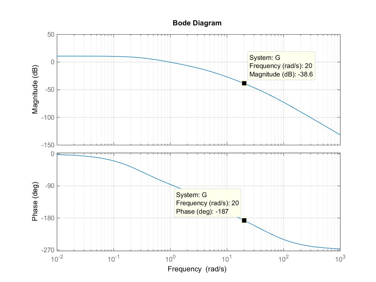
Let’s pick the values of [latex]\Phi_{m(comp)} = 55^{\circ}[/latex] and [latex]\omega_{cp(comp)}[/latex] rad/sec, and [latex]a_0=24.25[/latex] Next, the appropriate Controller parameters and clearly write the Lead Controller transfer function, [latex]G_c(s)[/latex]. We will use the analytical design formulae, but first we need to compute open loop gain and phase values at the chosen frequency of the crossover – we will use Matlab to obtain accurate values, as reading them off the graph may be too rough; see if you can read off the value close to -40 dB directly off the open loop Bode plot in Figure 13‑12. Matlab values are shown in Figure 13‑14.
[latex]\omega_{cp(comp)}=20rad/sec\rightarrow \left | G(j20) \right | = -38.6dB[/latex]
[latex]\left | G(j20) \right | = 0.0118[/latex]
[latex]\angle G(j\omega) = -186.9^{\circ}[/latex]
We can now compute the “lift” angle:
[latex]\theta=-180^{\circ}+\Phi_m-\angle G(j20)[/latex]
[latex]\theta=-180^{\circ}+55^{\circ}+187^{\circ}=62^{\circ}[/latex]
Apply the formulae:
[latex]a_1 = \frac{1-a_0\cdot \left | G(j\omega_{cp}) \right | \cdot \cos\theta}{\omega_{cp}\cdot \left | G(j\omega_{cp}) \right | \cdot \sin\theta} = \frac{1-28.34\cdot0.0118\cdot\cos62^{\circ}}{20\cdot0.0118\sin62^{\circ}} = 4.05[/latex]
[latex]b_1 = \frac{\cos\theta-a_0\cdot \left | G(j\omega_{cp}) \right |}{\omega_{cp}\cdot \sin\theta} = \frac{\cos62^{\circ}-28.34\cdot0.0118}{20\cdot\sin62^{\circ}} = 0.0077[/latex]
[latex]G_c(s)=\frac{a_1s+a_0}{b_1+1}=\frac{4.05s + 28.34}{0.0077s + 1}[/latex]
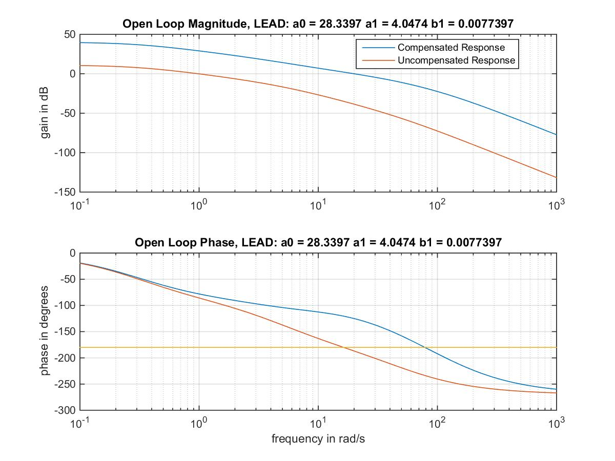
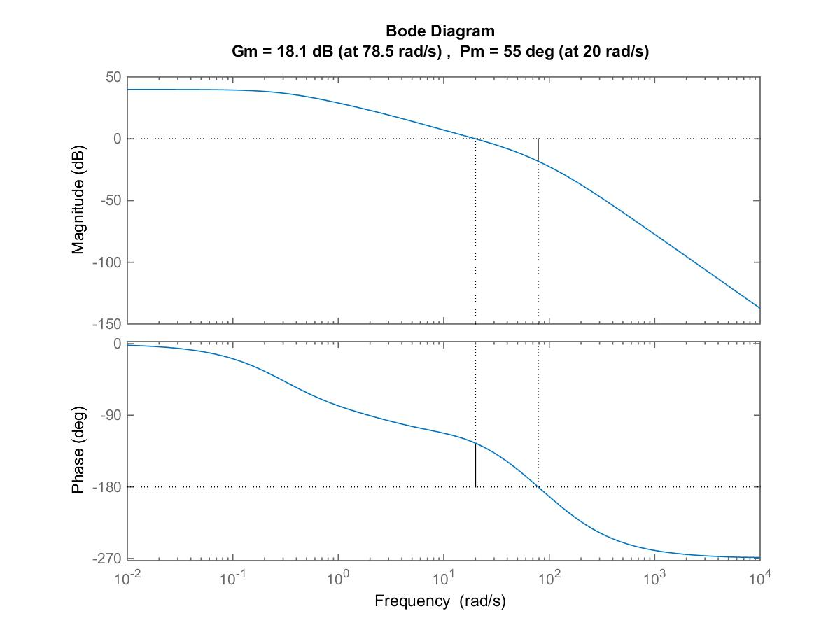
The Lead Controller transfer function coefficients are both positive, so the transfer function is acceptable! Let’s have a look at the compensated vs. uncompensated open loop Bode plots in Figure 13‑15. You can clearly see the characteristic shape of the open loop compensation – the increased open loop DC gain, the increased Phase Margin and crossover frequency. We can check the obtained values by using the “margin” function in Matlab, as shown in Figure 13‑21.
[latex]\Phi_{m_c} = 55^{\circ}[/latex] and [latex]\omega_{cp_c} = 20rad/sec[/latex]
Next, estimate the compensated closed loop step response specs: PO, [latex]e_{ss(step\%)}[/latex], [latex]T_{rise(0-100\%)}[/latex], and [latex]T_{settle(\pm2\%)}[/latex].
The estimated specs are going to be as expected since we created the compensated closed loop system model based on these:
[latex]\zeta = 0.5169[/latex], [latex]\omega_n = 25.8[/latex], [latex]K_{dc} = 0.99[/latex]
[latex]G_{mc}(s)=\frac{658.6}{s^2 + 26.67s + 665.3}[/latex]
Thus, we expect these estimates, as per model:
[latex]PO = 100\cdot\left ( e^{\frac{-\zeta\pi}{\sqrt{1-\zeta^2}}} \right )=15\%[/latex]
[latex]T_{settle(\pm2\%)}=\frac{4}{\zeta\omega_n}=0.3[/latex]
[latex]T_{rise(0-100\%)} = \frac{\pi-cos^{-1}\zeta}{\omega\sqrt{1-\zeta^2}}=0.1[/latex]
[latex]e_{ss(step)}= 1 - K_{dc}=1-0.99=0.01[/latex], [latex]e_{ss(step\%)}= 1\%[/latex]
Let’s now check if the closed loop response conforms to these expectations. The compensated open loop system transfer function is:
[latex]G_{open(c)}(s)=\frac{4.05s + 28.34}{0.0077s + 1}\cdot \frac{262}{(s+0.3)(s + 5)(s+50)}[/latex]
The closed loop system transfer function is:
[latex]G_{cl(c)}(s)=\frac{\frac{4.05s + 28.34}{0.0077s + 1}\cdot\frac{262}{(s+0.3)(s+5)(s+50)}}{1 + \frac{4.05s + 28.34}{0.0077s + 1}\cdot \frac{262}{(s+0.3)(s+5)(s+50)}}[/latex]
[latex]G_{cl(c)}(s)=\frac{68254(s+7)}{(s+139.9)(s+7.78)(s^2+36.77s+890)}[/latex]
The dominant pair of complex poles is at: [latex]-18.4 \pm j 23.5[/latex]. Based on the closed loop transfer function, we can expect a near-pole-zero cancellation weakening the effect on the significant pole-zero pair at -7 and -7.78 respectively; the pole at -139.9 is not insignificant either but it should counteract the effect of the not-entirely cancelled zero. Conclusion – the actual compensated system response should be very similar to the predicted model. This is confirmed by the plots in Figure 13‑17. The actual system response, despite the presence of an extra pole and an extra zero, is not that different from the expected response, confirming the validity of this approach.
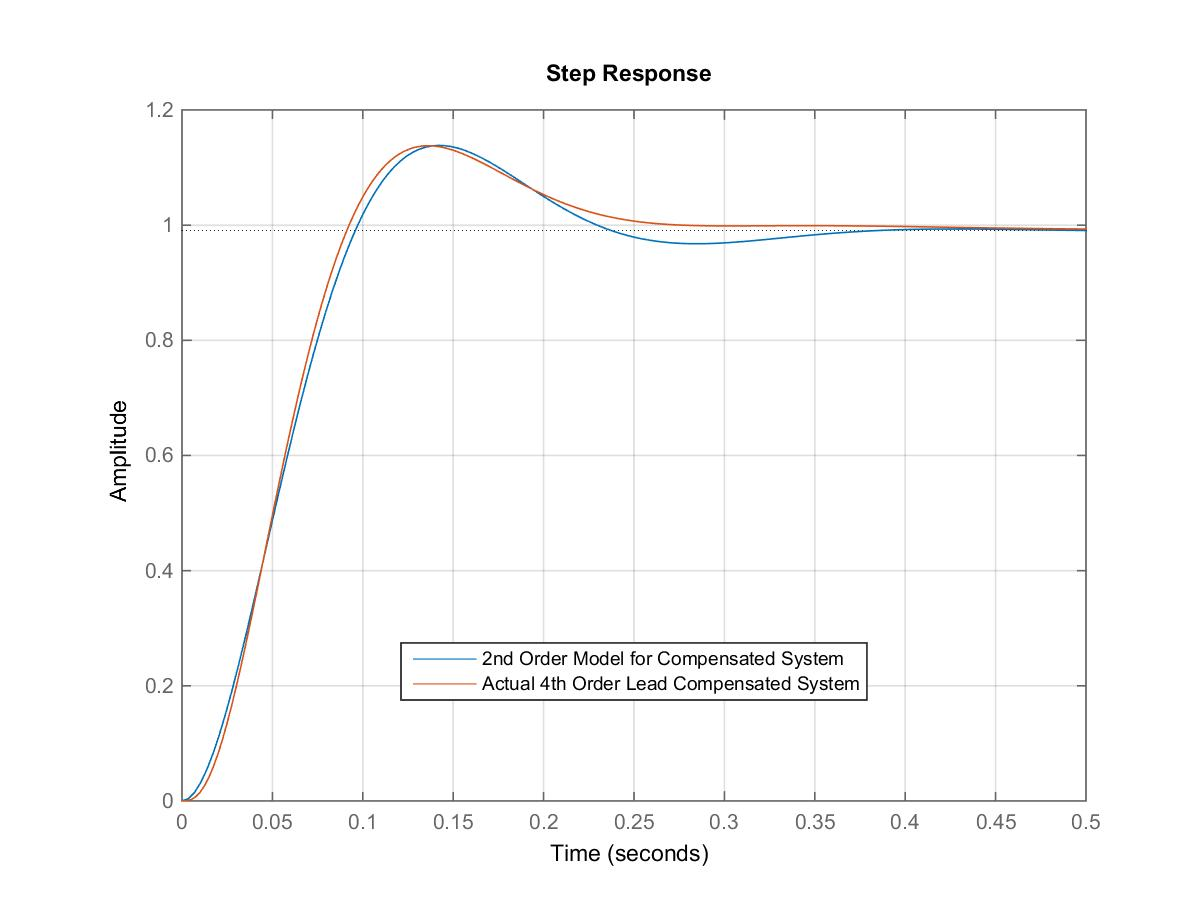
Below, we compare the expected specs, based on the model, with the actual system response specs, obtained by running the “stepeval” function. The actual specs, compared to the model specs, are:
| Actual Compensated
System |
[latex]G_{mc}(s)[/latex] – Model for the Compensated System |
|
| PO | 14.9% | 15% |
| [latex]e_{ss(step\%)}[/latex] | 1% | 1% |
| [latex]T_{rise(0-100\%)}[/latex] | 0.093 sec | 0.1 sec |
| [latex]T_{settle(\pm2\%)}[/latex] | 0.24 sec | 0.3 sec |
The specs estimates from the model are very accurate, with all specs meeting the required values.
