Chapter 13
13.5 Lag Controller Design – Solved Example 1
Consider a typical unit feedback closed loop control system, as shown, which is to operate under Lag Control.

The Lag Controller transfer function is as follows:
[latex]G_c(s)=K_c\cdot\frac{\tau\alpha s +1}{\tau s+1}=\frac{a_1 s +a_0}{b_1 s+1}[/latex]
Where [latex]\tau[/latex] is the so-called Lag Time Constant and [latex]\alpha = 1[/latex]. The process transfer function G(s) is:
[latex]G(s)=\frac{30(s+2)}{{(s+0.1)}^2 {(s+20)}^2}[/latex]
Open loop frequency response plots of G(s) are shown in Figure 13‑20. The closed loop performance requirements are: the Steady State Error for the unit step input for the compensated closed loop system is one half of the Steady State Error for the uncompensated system; Percent Overshoot is approximately 10%.
Check what the current (uncompensated system) values of the Phase Margin, [latex]\Phi_m[/latex], and the Crossover Frequency, [latex]\omega_{cp}[/latex] are. Estimate the uncompensated closed loop step response specs: Percent Overshoot, PO, Steady State Error, [latex]e_{ss(step\%)}[/latex], and Settling Time, [latex]T_{settle(\pm2\%)}[/latex]. Next, based on the specifications, calculate the required values of the Phase Margin for the compensated system, [latex]\Phi_{mc}[/latex], and the DC gain of the controller, [latex]K_{dc}[/latex].
Design the Lag Controller such that it meets the closed loop response requirements, and write the Lag Controller transfer function and its parameters. For your Controller, estimate the compensated closed loop step response specs: Percent Overshoot, PO, Steady State Error, [latex]e_{ss(step\%)}[/latex], Rise Time, [latex]T_{rise(100\%)}[/latex], and Settling Time, [latex]T_{settle(\pm2\%)}[/latex].
Let’s start by finding the open loop DC gain – note that reading the gains off the Bode plots is difficult due to decibel units – here the gain could be read off from Figure 13‑20 as anywhere between 20 and 25 dB. It is recommended to always use the transfer function (if available) to compute the accurate gain values. Here we can compute the Uncompensated Open Loop DC gain – there is no controller, i.e. [latex]G_c(s) = 1[/latex].
From the process transfer function:
[latex]K_{dco}=\lim_{s\rightarrow0}\frac{30(s+2)}{{(s+0.1)}^2{(s+20)}^2}=\frac{60}{4}=15[/latex]

The uncompensated closed loop DC gain is then:
[latex]K_{dc} = \frac{K_{dco}}{1+K_{dco}}=\frac{15}{16}=0.9375[/latex]
The Phase Margin and the crossover frequency can be read off from the Bode plot in Figure 13‑20 as: [latex]\Phi_m = 38^{\circ}[/latex] and [latex]\omega_{cp} = 0.378[/latex] rad/sec. The damping ratio [latex]\zeta[/latex] and the frequency of natural oscillations [latex]\omega_n[/latex] for the uncompensated closed loop system can now be estimated by either reading it off the Phase Margin graph in Figure 12‑9 or by using the formula: [latex]\zeta = 0.3487[/latex]. Next, calculate the natural frequency:
[latex]\omega_n = \frac{\tan{\Phi_m}\cdot\omega_{cp}}{2\zeta}=0.426[/latex]
The uncompensated closed loop model:
[latex]G_m(s)=K_{dc}\frac{\omega_n^2}{s^2+2\zeta\omega_n s + \omega_n^2} \rightarrow G_{mu}(s)=\frac{0.1701}{s^2+0.2971 s + 0.1814}[/latex]
Model specs can be calculated as:
[latex]PO = 100\cdot \left ( e^{\frac{-\zeta\pi}{\sqrt{1-{\zeta}^2}}} \right ) = 31\%[/latex]
[latex]T_{settle(\pm2\%)}=\frac{4}{\zeta\omega_n}=26.9[/latex]
[latex]T_{rise(100\%)}=\frac{\pi-\cos\zeta^{-1}}{\omega_n\sqrt{1-\zeta^2}}=4.82[/latex]
[latex]e_{ss(step\%)}=\frac{1}{1+K_{pos}}\cdot100\%=\frac{1}{1+15}=6.25\%[/latex]
The actual closed loop uncompensated transfer function is:
[latex]G_{cl}(s)=\frac{30s + 60}{s^4 + 40.2s^3 + 408s^2 + 110.4s +64}[/latex]
[latex]G_{cl}(s)=\frac{30(s+2)}{(s+21.14)(s+18.8)(s^2 + 0.262s + 0.161)}[/latex]
As we can see, the closed loop transfer function has a dominant pair of complex poles, with the damping ratio [latex]\zeta = 0.326[/latex] and the natural frequency of oscillations [latex]\omega_n = 0.4[/latex] rad/sec, which are very close to the model estimates of [latex]\zeta = 0.349[/latex] and [latex]\omega_n = 0.426[/latex] rad/sec. The actual transfer function also has a zero at -2, and two poles at – 21.14 and -18.8, all of which are negligible, compared to the dominant pair of closed loop poles located at [latex]-0.13\pm j0.38[/latex]. Thus, the assumed model is quite accurate – see the actual step response comparison, shown in Figure 13‑21.
Below, we compare the expected specs, based on the model, with the actual system response specs, obtained by running the “stepeval” function. The actual specs, compared to the model specs, are:
| Actual Compensated System | [latex]G_{mc}(s)[/latex] – Model for the Compensated System | |
| PO | 54.8% | 31% |
| [latex]e_{ss(step\%)}[/latex] | 6.25% | 6.25% |
| [latex]T_{rise(0-100\%)}[/latex] | 4.68 sec | 4.82 sec |
The specs estimates from the model are very accurate, with all specs meeting the required values.

Now, the Lag Controller design – we can choose a simplified design or an analytical design. First, always calculate the required DC gain of the controller – this part is the same in both approaches. Based on the required error specification:
[latex]e_{ss(step)c}=0.5\cdot e_{ss(step)u} \rightarrow \frac{1}{K_{posu}}=\frac{0.5}{1+K_{posu}}[/latex]
[latex]\frac{1}{K_{posu}}=\frac{0.5}{1+K_{posu}} \rightarrow k_{posu}=31[/latex]
The compensated closed loop DC gain should be:
[latex]K_{dc(comp)}=\frac{K_{posc}}{1+K_{posc}}=\frac{31}{32}=0.9688[/latex]
The controller DC gain is then:
[latex]K_c = a_0 = \frac{K_{posc}}{K_{posu}}=\frac{31}{15}=2.067[/latex]
Next, “translate” the required PO spec into the equivalent closed loop damping ratio. Based on Figure 7‑4, for PO = 10%, the required damping ratio is approximately [latex]\zeta =0.59[/latex]. The compensated Phase Margin, based on Figure 12‑9 should be close to [latex]\Phi_{m(comp)} = 60^{\circ}[/latex].
What do we do next? The two approaches differentiate on how we proceed.
13.5.1.1 Lag Controller Design Solved Example 1: The “Simplified” Lag Design
Recall that at the frequency of [latex]\frac{10}{\alpha\tau}[/latex] in the Lag Controller (see the graph below), we are still losing about of [latex]5^{\circ}[/latex] phase, so look at the uncompensated open loop Bode plot and choose the frequency where the phase angle is ([latex]\Phi_m + 5^{\circ}[/latex]) away from the [latex]-180^{\circ}[/latex] line. Here, if we want the compensated Phase Margin to be [latex]\Phi_m = 60^{\circ}[/latex], we should look for the frequency where the phase angle reaches [latex]-115^{\circ}[/latex]:
[latex]\angle G(j\omega) = -180^{\circ}+\Phi_m + 5^{\circ} = -180^{\circ}+60^{\circ} + 5^{\circ}[/latex]
That frequency is read off the plot as approximately 0.17 rad/sec: [latex]\omega_{co(comp)} = 0.17[/latex] rad/sec. Note that in the Lag Design, the compensated crossover frequency will always be to the left of the uncompensated frequency of the crossover. If it were to the right of the uncompensated frequency of the crossover, we would end up with a Lead Design. Here the uncompensated frequency is 0.38 rad/s. Next, find the gain of the uncompensated system at that point – recall that reading it off the graph is inaccurate so it is best to substitute [latex]s = j0.17[/latex] into G(s):
[latex]\left | G(j0.17) \right | = 3.87\frac{V}{V}=11.75dB[/latex]

Remember that since we are using the DC gain of 2.0667, the total gain at the chosen crossover frequency is going to be 3.87 times 2.0667. This is the amount of the gain reduction that has to be delivered by the high frequency gain drop-off of the Lag Controller:
[latex]\alpha = \frac{1}{2.0667\cdot3.87}=0.125[/latex]
[latex]\omega_{cp(comp)}[/latex] rad/sec becomes the right-side corner of the phase characteristic:
[latex]\omega_{cp(comp)}=0.17=\frac{10}{\alpha\tau} [/latex]
[latex]\tau = \frac{10}{\alpha\cdot\omega_{cp}}=\frac{10}{0.125\cdot0.17}=4704[/latex]
The controller transfer function is:
[latex]G_c(s)=K_c\cdot\frac{\tau\alpha s + 1}{\tau s + 1}=2.0647\cdot\frac{470.4\cdot0.125s+1}{470.4s+1}=2.0647\cdot\frac{58.82s+1}{470.4s+1}[/latex]
[latex]G_c(s)=\frac{a_1 s + a_0}{b_1 s +1 }= \frac{121.6s+2.067}{470.4s+1} [/latex]
The open loop Bode plots before and after compensation and the system Phase Margin are shown in Figure 13‑22 and the compensated Phase Margin is shown in Figure 13‑23 – it is [latex]\Phi_m=60^{\circ}[/latex] at the frequency of [latex]\omega_{cp(comp)}=0.17[/latex] rad/sec, as was chosen for this design.


The expected compensated closed loop response specs can be estimated using the dominant poles model again. Use the formula below, or read off the Phase Margin graph in Figure 12‑9:
[latex]\zeta=\frac{\tan{\Phi_m}}{2\sqrt{{(\tan\Phi_m)}^2 + 1}} \rightarrow \zeta = 0.607[/latex]
[latex]\omega_n = \frac{\tan{\Phi_m}\cdot\omega_{cp}}{2\zeta} = 0.24[/latex]
The compensated closed loop model:
[latex]G_{mc}(s)=\frac{0.054}{s^2 + 0.291s + 0.054}[/latex]
Model specs can be calculated as:
[latex]PO=100\cdot\left ( e^{\frac{-\zeta\pi}{\sqrt{1-\zeta^2}}} \right )=9\%[/latex]
[latex]T_{settle(\pm2\%)}=\frac{4}{\zeta\omega_n}=27.4[/latex]
[latex]T_{rise(100\%)}=\frac{pi-\cos\zeta^{-1}}{\omega_n\sqrt{1-\zeta^{2}}}=11.5[/latex]
[latex]e_{ss(step\%)}=\frac{1}{1+K_{pos}}\cdot100\%=\frac{1}{1+31}\cdot100\%=3.125\%[/latex]
The actual closed loop transfer function is:
[latex]G_{cl}(s)=\frac{7.753(s+2)(s+0.017)}{(s+20.59)(s+19.4)(s+0.01463)(s^2 + 0.203s + 0.047)}[/latex]
As we can see, the actual closed loop transfer function has a dominant pair of complex poles, with the damping ratio [latex]\zeta=0.47[/latex] and the natural frequency of oscillations [latex]\omega_n = 0.22[/latex] rad/sec, as well as a zero at -2, another zero at -0.017, and three real poles at – 20.59, -19.4 and at -0.01463.
The dominant poles model is not as accurate as before, because now an additional pole-zero combo shows up, and both are very close to the Imaginary axis. They do not cancel out, and their net effect on the closed loop response is that the very large time constant associated with the Lag Controller causes a very slow, very visible exponential component in the step response – see the actual step response comparison in Figure 13‑24 and the comparison of the specs below. That additional real pole has a very long decay time associated with it, which significantly affects the Settling Time.
Below, we compare the expected specs, based on the model, with the actual system response specs, obtained by running the “stepeval” function. The actual specs, compared to the model specs, are:
| Actual Compensated System | [latex]G_{mc}(s)[/latex] – Model for the Compensated System | |
| PO | 4.6% | 9% |
| [latex]e_{ss(step\%)}[/latex] | 3.125% | 3.125% |
| [latex]T_{rise(0-100\%)}[/latex] | 14.1 sec | 11.5 sec |
| [latex]T_{settle(\pm2\%)}[/latex] | 130.4 sec | 24.8 sec |
Clearly, the biggest problem with the simplified approach is that it typically generates a long-time constant that causes the closed loop system to have the real pole close to the Imaginary axis that cannot be ignored – the closed loop model is not really based on a dominant pair of complex poles alone. Unfortunately, the simplified design does not allow us to avoid this. Let’s consider the analytical design next.
Plus of the simplified design – it will never lead to negative values of the controller parameters.
Minus of the simplified design – it almost always results in an additional significant closed loop pole that has a strong negative effect on the Settling Time. This can be somehow ameliorated by trial & error adjustments, but it would be tedious.

13.5.1.2 Lag Controller Design Solved Example 1: The “Analytical” Lag Design
The analytical design gives us more flexibility to shape the open loop response by choosing different locations for the crossover frequency. Remember to choose the required DC gain based on the error specs – the calculations are identical to the simplified method, so the Controller DC gain ([latex]a_0[/latex]) will be the same:
[latex]e_{ss(step)c}=0.5\cdot e_{ss(step)u} \rightarrow\frac{1}{1+K_posc}=\frac{0.5}{1+K_{posu}}[/latex]
[latex]\frac{1}{1+K_{posc}}=\frac{0.5}{1+15}\rightarrow K_{posc}=31[/latex]
The compensated closed loop DC gain should be:
[latex]K_{dc(comp)}=\frac{K_{posc}}{1+K_{posc}}=\frac{31}{32}=0.9688[/latex]
The controller DC gain is again:
[latex]a_0=\frac{K_{posc}}{K_{posu}}=\frac{31}{15}=2.067[/latex]
Next, we pick the Phase Margin – in this example, we decided to have the Phase Margin of [latex]60^{\circ}[/latex], so let’s stick with this value. Next, we need to choose the crossover frequency – as long as it is less than 0.38 (the uncompensated value). First, let’s choose the same value as in the simplified design:
[latex]\omega_{cp(comp)}=0.17 rad/sec[/latex]
To use the derived formulae for the controller constants [latex]a_1[/latex] and [latex]b_1[/latex], we need to calculate the uncompensated open loop Bode plot the phase and the gain at that frequency – as before, substitute [latex]s=j0.17[/latex] into the transfer function G(s):
[latex]\angle G(j0.17)=-115^{\circ}[/latex]
[latex]\left | G(j0.17) \right | = 3.87\frac{V}{V}=11.75dB[/latex]
Next, substitute these values into the formulae:
[latex]\theta=-180^{\circ}+\Phi_m-\angle G(j0.17)= -180^{\circ}+60^{\circ}+115^{\circ} = -5^{\circ}[/latex]
Note since this is a LAG design, the “lift” angle is not really “lifting” anything; it is just an intermediate step in the calculation and could be even called a “drag” or “lag” angle. Also note this calculation confirms our assumption in the “simplified” design that at the chosen crossover frequency, we are losing approximately 5 degrees of phase to the lag controller.
[latex]a_1 = \frac{1-a_0\cdot\left | G(j\omega_{cp})\right | \cdot \cos \theta}{\omega_{cp}\cdot\left | G(j\omega)\right |\cdot\sin\theta}=126.2[/latex]
[latex]b_1 = \frac{\cos\theta-a_0\cdot\left | G(j\omega_{cp})\right | }{\omega_{cp}\cdot\sin\theta}=490.6[/latex]
These values are very close to the ones obtained using the simplified approach, as expected. The closed loop response will also be similar, with the large value of the closed loop time constant dominating the response and adversely affecting the Settling Time. The resulting design offers some improvement over the uncompensated response, but the Settling Time spec takes a huge beating – this is not a good design and we should be able to do better.
With the analytical design we are not stuck with the one choice of the crossover frequency, as is the case with the simplified design. We can easily choose a different frequency of the crossover (as long as it is less than the uncompensated crossover frequency) and see if the resulting closed loop step response simulations will improve. Let’s consider what would happen if we chose a different value for the crossover frequency. Let’s say, make [latex]\omega_{cp(comp)}=0.2[/latex] rad/sec. Again, we need to find the gain of the uncompensated system at that point – recall that reading it off the graph is inaccurate so it is best to substitute [latex]s=j0.2[/latex] into G(s):
[latex]\angle G(j0.2) = -122^{\circ}[/latex]
[latex]\left | G(j0.2) \right | = 3.01\frac{V}{V}=9.6dB[/latex]
Next, substitute these values into the formulae:
[latex]\theta = -180^{\circ} + \Phi_m - \angle G(j0.2)= -180^{\circ}+60^{\circ}+122^{\circ}=2^{\circ}[/latex]
[latex]a_1 = \frac{1-a_0\cdot\left | G(j\omega_{cp})\right | \cdot \cos \theta}{\omega_{cp}\cdot\left | G(j\omega)\right |\cdot\sin\theta}=-215.5[/latex]
[latex]b_1 = \frac{\cos\theta-a_0\cdot\left | G(j\omega_{cp})\right | }{\omega_{cp}\cdot\sin\theta}=-650.3[/latex]
[latex]G_c(s)=\frac{a_1 s + a_0}{b_1 s +1}=\frac{-215.5s + 2.067}{-650.3s +1}[/latex]
So here we have an unpleasant surprise! The controller coefficients are not acceptable, as they are negative! The controller pole in RHP is unacceptable because it means an unstable open loop transfer function – even if the resulting closed loop is stable, for safety reasons we do not want to implement that – in case if the closed loop incidentally opens (a malfunction), we would have an unstable system on our hands. The RHP location of the controller zero is also unacceptable. Even if the controller pole is in a stable location, the RHP zero will introduce an effective delay into the system, extending both the Rise Time and the Settling Time. Recall that we will never get that kind of surprise in the “simplified” lag design.
Let’s keep adjusting the value of the crossover frequency – we already have one “passable” value, at 0.17 rad/sec, but we want to improve on that design. By “trial & error” we find that values of crossover frequency that are between 0.19 and 0.38 all result in negative coefficients and are therefore unacceptable. Let’s try frequencies smaller than 0.17 – some of those choices will lead to acceptable controller values. Let’s see if we can get a set of controller values that would give us a better actual step response than the one seen above for [latex]\omega_{cp(comp)} = 0.17 rad/sec[/latex] – remember that one was quite different from expected because it had a large time constant associated with the Lag controller.
After some trial & error with the analytical formulae, we come across quite an agreeable response – note that the formulae can be easily programmed into Matlab so that the iterations are quite easy to perform. Let’s see the results for [latex]\omega_{cp(comp)} = 0.1 rad/sec[/latex] – good results can be had for some other, smaller values as well. Again, we need to find the gain and phase of the uncompensated system at that frequency – recall that reading it off the graph is inaccurate so it is best to substitute [latex]s=j0.1[/latex] into G(s):
[latex]\angle G(j0.1)=-88^{\circ}[/latex]
[latex]\left | G(j0.1) \right | = 7.5\frac{V}{V}=17.5dB[/latex]
Next, substitute these values into the formulae and first calculate our “lag” angle:
[latex]\theta = -180^{\circ}+\Phi_m-\angle G(j0.1)=-180^{\circ}+60^{\circ}+88^{\circ}=-32^{\circ}[/latex]
Note that at this point the “lift” angle has become a “lag” angle (negative value).
[latex]a_1 = \frac{1-a_0\cdot\left | G(j\omega_{cp})\right | \cdot \cos \theta}{\omega_{cp}\cdot\left | G(j\omega)\right |\cdot\sin\theta}=30.2[/latex]
[latex]b_1 = \frac{\cos\theta-a_0\cdot\left | G(j\omega_{cp})\right | }{\omega_{cp}\cdot\sin\theta}=274.7[/latex]
Both controller parameters are positive, so this controller will be acceptable. The open loop Bode plots before and after compensation are shown in Figure 13‑25 and the system Phase Margin is shown in Figure 13‑26.

The controller transfer function is:
[latex]G_c(s)=\frac{a_1 s + a_0}{b_1 s + 1}=\frac{30.2s+2.067}{274.7s+1}[/latex]
Note that with a much smaller value of [latex]b_1[/latex], this design may be actually better than the one with a higher crossover frequency, as the closed loop compensated response will be closer to the expected model – no slow exponential visible. Let’s check this theory out. The expected compensated closed loop response can be estimated using the dominant poles model again. Use the formula below, or read off the Phase Margin graph in Figure 12‑9:
[latex]\zeta = \frac{\tan\Phi_m}{2\sqrt{\sqrt{{(\tan\Phi_m)}^2 + 1}}} \rightarrow \zeta = 0.612[/latex]
[latex]\omega_n = \frac{\tan\Phi_m\cdot\omega_{cp}}{2\zeta}=0.1414[/latex]

The compensated closed loop model:
[latex]G_{mc}(s)=\frac{0.0194}{s^2+0.173s+0.02} [/latex]
Model specs can be calculated as:
[latex]PO = 100\cdot \left ( e^{\frac{-\zeta\pi}{\sqrt{1-{\zeta}^2}}} \right ) = 9\%[/latex]
[latex]T_{settle(\pm2\%)}=\frac{4}{\zeta\omega_n}=46.2[/latex]
[latex]T_{rise(100\%)}=\frac{\pi-\cos\zeta^{-1}}{\omega_n\sqrt{1-\zeta^2}}=20[/latex]
[latex]e_{ss(step\%)}=\frac{1}{1+K_{pos}}\cdot100\%=\frac{1}{1+31}=3.125\%[/latex]
The actual closed loop transfer function:
[latex]G_{cl}(s)=\frac{3.3(s+2)(s+0.068)}{(s+20.38)(s+19.6)(s+0.063)(s^2 + 0.1469s +0.0184)}[/latex]
Note that the closed loop model based on the dominant poles is now more accurate than in the case of the “simplified” design – while the additional pole-zero combo still shows up, both very close to the Imaginary axis, their net effect on the closed loop response is almost negligible because of a much better “near-cancellation”: we have a zero at -0.068, and a pole at -0.063. Before they were at -0.017 and -0.0146, respectively. The very large time constant associated with the Lag Controller is no longer visible in the step response, and the Settling Time is much as expected – see the actual step response comparison and the comparison of the specs below.
Below, we compare the expected specs, based on the model, with the actual system response specs, obtained by running the “stepeval” function. The actual specs, compared to the model specs, are:
| Actual Compensated System | [latex]G_{mc}(s)[/latex] – Model for the Compensated System | |
| PO | 10.6% | 8.8% |
| [latex]e_{ss(step\%)}[/latex] | 3.125% | 3.125% |
| [latex]T_{rise(0-100\%)}[/latex] | 19.7 sec | 20.1 sec |
| [latex]T_{settle(\pm2\%)}[/latex] | 41.1 sec | 42.1 sec |
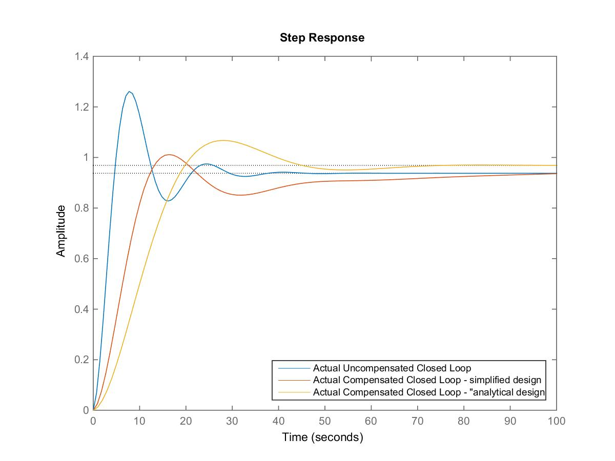
The estimates are very accurate. Finally, let’s see how much of an improvement we achieved by introducing the Lag Controller – see the comparison of the responses in Figure 13‑28.
Plus of the Analytical Lag Design – it can be quickly iterated to find a much better system performance, often without the long and visible slow time constant associated with the Simplified Lag Design.
Minus of the Analytical Lag Design – sometimes the design formulae will yield negative, i.e. unacceptable, values of controller parameters. This can be addressed by a slightly different choice of the crossover frequency and the phase margin.